Silicon Photonics Explained: Why Light Will Replace Copper Interconnects in AI Clusters
As frontier AI clusters demand multi-gigawatt power, traditional copper interconnects have hit a physical thermal wall. Here is how co-packaged optics (CPO) and laser waveguides are revolutionizing data center physics.

Reach 50,000+ Tech Enthusiasts, Developers & Innovators
Google AdSense & Direct Partner Sponsorship Slot Reserved for techdaur.com
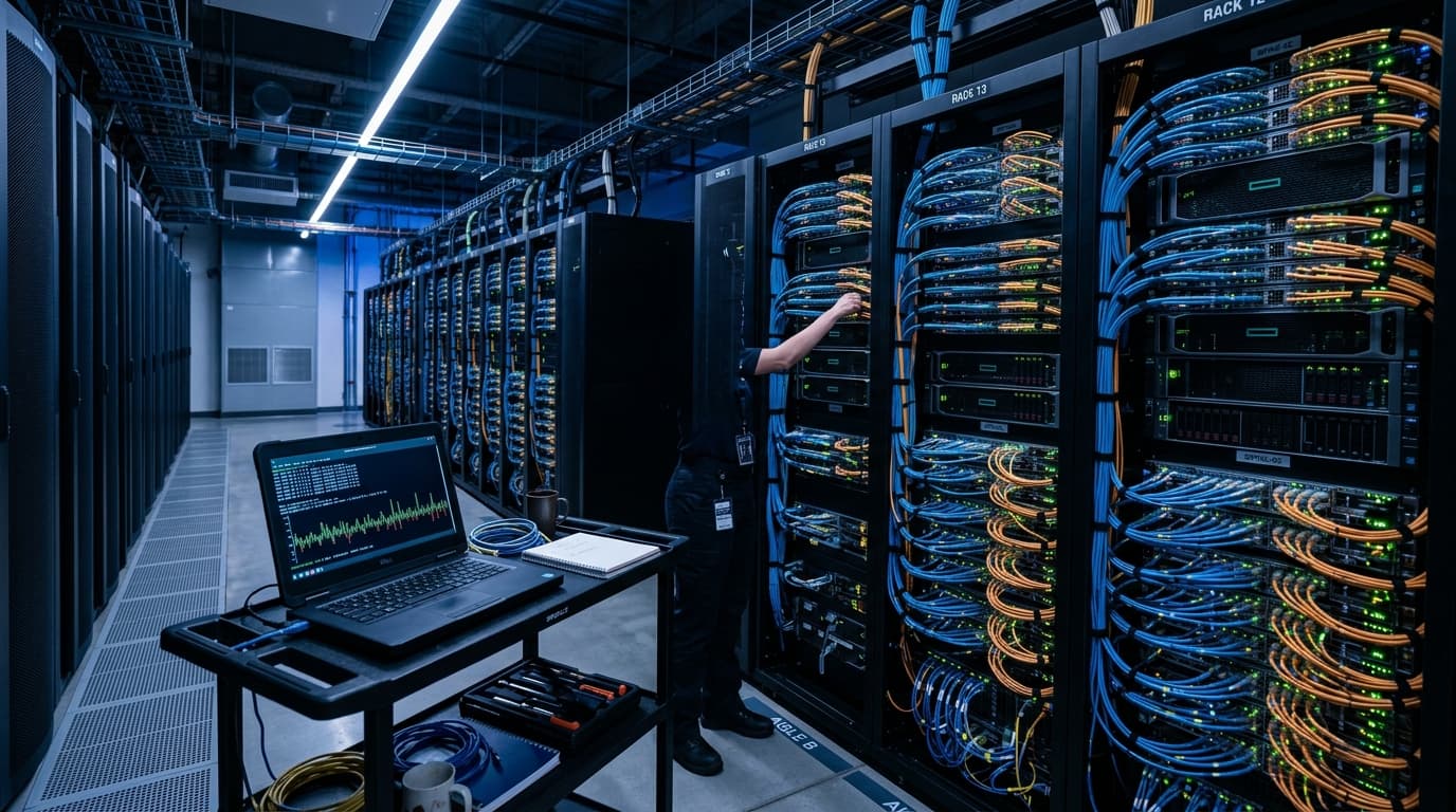
Co-Packaged Optics (CPO) Silicon Architecture
The Pros
- ✓Delivers 10x higher bandwidth density compared to passive copper cables at 800Gbps and 1.6Tbps
- ✓Reduces server rack power dissipation by up to 35%, preventing catastrophic thermal throttling
- ✓Enables multi-kilometer optical fabric scaling without requiring active electrical signal repeaters
The Cons
- —High laser diode manufacturing defect rates currently challenge packaging yields
- —Commercial data center transition cycles take 18 to 24 months for hyperscalers to retool
Key Takeaways
- •Copper cables experience severe capacitive attenuation at frequencies above 200GHz per lane.
- •Co-Packaged Optics (CPO) mounts microscopic optical engines directly onto the same substrate as the GPU.
- •Switching from electrical to optical signaling slashes data center energy loss by hundreds of megawatts.
The Physical Impedance Wall of Copper Wires
For over fifty years, the computing industry relied on copper traces and cables to move electrons between chips. As long as speeds were modest, copper was cheap, malleable, and reliable. But in the era of multi-trillion parameter AI training runs, thousands of GPUs must exchange tens of terabytes of tensor weights every millisecond. At speeds of 800Gbps and 1.6Tbps, electrons in copper encounter severe high-frequency skin effects and dielectric losses. Over 60% of the energy consumed by high-speed copper interconnects is dissipated as useless, dangerous heat.
Reach 50,000+ Tech Enthusiasts, Developers & Innovators
Google AdSense & Direct Partner Sponsorship Slot Reserved for techdaur.com
How Silicon Photonics Operates at the Nanoscale
Silicon photonics solves this dilemma by converting electrical signals into pulses of infrared light inside microscopic optical waveguides carved directly into standard silicon wafers. Because light waves do not generate electromagnetic interference and experience virtually zero capacitive attenuation, photons can travel kilometers through microscopic glass fibers with negligible energy loss. By integrating micro-ring modulators and photodetectors, chips can transmit hundreds of optical channels simultaneously using Wavelength Division Multiplexing (WDM).
Co-Packaged Optics (CPO): The End of Pluggable Transceivers
Until recently, data centers used pluggable optical transceivers mounted on the faceplates of switch chassis. While convenient, the electrical signal still had to travel several inches across the motherboard from the processor to the transceiver, wasting valuable power. Co-Packaged Optics (CPO) physically bonds the optical transceiver engine directly onto the same advanced packaging interposer (such as TSMC's CoWoS) right next to the compute silicon. This shrinks electrical trace lengths from inches to millimeters, cutting signal energy expenditure by over 70%.
Frequently Asked Questions
Why can't silicon itself emit light efficiently?
Silicon has an indirect bandgap, meaning electrons cannot easily drop energy levels to release photons; therefore, hybrid lasers use Indium Phosphide (InP) bonded onto silicon.
When will silicon photonics be standard in consumer computers?
Silicon photonics will dominate hyperscale AI data centers first (2026–2028) before trickling down into high-end workstation motherboards by the end of the decade.
Almas
Silicon architecture researcher and semiconductor analyst tracking next-generation lithography and computing physics.
More from TechDaur
Inside the 2nm Silicon Revolution: How GAAFET Transistors Are Rescuing Moore's Law
Stay Ahead in Tech & AI
Join 15,000+ developers, engineers, and creators. Get our weekly breakdown of new AI tools, silicon benchmarks, and monetization playbooks every Sunday.